Monday, February 16, 2009

Basic Op Amp Model

Basic Op Amp Model

CIRCUIT

OPMODEL1.CIR Download the SPICE file

One of the challenges of simulating opamp circuits is modeling the op amp itself. How is that accomplished? There's a couple of ways. You can create a circuit of many transistors, resistors and caps that closely replicate the internals of an op amp. Or, you can create a simpler model that reproduces the basic behavior of the op amp. The benefit of the simpler model is one that uses less components and typically simulates faster. As you begin to look at more complex or subtle behaviors, you can create a more complex op amp model.

To simulate more complex behaviors, check out the Intermediate Op Amp Model. For a description of all available op amp models, see Op Amp Models.
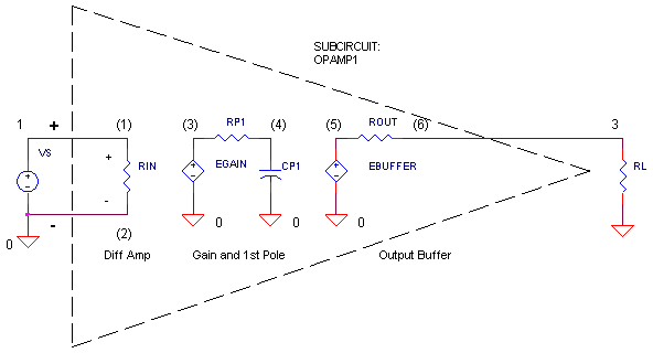
OP AMP MODEL

What are the three basic stages of an op amp? The circuit above shows 1) a differential amplifier, 2) a voltage gain stage with single-pole frequency roll-off and 3) an output buffer. (As a convenience, we'll define this model as a subcircuit. See Why Use Subcircuits?)

The subcircuit models the following behaviors:

Input impedance RIN
Differential Gain EGAIN
Single Pole Frequency RP1, CP1
Output Impedance ROUT

If you're designing a precision amplifier, you can see how gain and input / output resistance effect accuracy. If your designing a high-speed amplifier, you can determine your circuit's bandwidth. You can also see how stray and load capacitances may cause your amplifier to ring or oscillate.

OPEN-LOOP FREQUENCY RESPONSE

The open-loop response gives you some powerful insight into the op amp’s performance. Open-loop means NO feedback; the response of the “naked” op amp. Two important features are

1. DC Gain – the gain at DC. ( The more you have, the more accurate your amplifier. )

2. First-Pole Frequency, fp1 – the frequency where the open-loop begins to fall. A direct result of fp1 and the DC Gain is the Unity-Gain Frequency, fu – the frequency where the open-loop gain falls to 1 V/V. The greater the fu, the faster your op amp can respond.

CIRCUIT INSIGHT The op amp is driven by AC source VS. There are no feedback resistors here – its running open-loop. Try out the model by running a simulation and plotting the AC magnitude VM(3). Can you see the DC gain = 100k V/V and the first-pole at fp1 = 100 Hz? What is the unity gain frequency? Try changing the Y-Axis to a log scale to get a better view at high frequencies. If your plotting in dB, the unity-gain level is 0 dB.

You might ask, what if I don’t need a gain of 100k V/V? Op amps are actually intended for lower gains set by feedback resistors connected around the device (Closed-Loop Gain). The higher the internal gain (like 100k V/V and above) the more accurate your lower Closed-Loop Gain will be (set by the feedback resistors only.)

UNITY-GAIN FREQUENCY

As stated before, the greater the unity-gain frequency, the faster your op amp can respond. What determines the this frequency? It’s set by the DC Gain and fp1.

where the pole frequency is formed by a simple RC filer

HANDS-ON DESIGN Suppose you need to model an op amp with the same DC gain but a higher unity-gain frequency fu. Simply solve for a new fp1 in the 1st equation. Then, calculate the new CP1 from the 2nd equation to achieve that desired fp1. For example,

Choose a new fu, such as 50 MHz.
Then, calculate fp1 = fu / DCGAIN = 50 MHz / 100 k = 500 Hz
CP1 = 1/( 2 *
π * 1k * 500 Hz) = 0.318 uF.

Try out your new op amp model. Did the magnitude VM(3) hit the unity-gain where you expected?

PHASE SHIFT

CIRCUIT INSIGHT So far we’ve looked at the gain / attenuation of the input signal by the op amp. At some point, you may need to know the phase shift (time shift) as well. To check out the phase shift, add another plot to the window, then, add trace VP(3) where the P tells SPICE to display the Phase. A maximum of -90 degrees of phase shift should occur beyond the first pole fp1.

What’s the big deal about phase anyway? Turns out, the phase shift (and gain) of the signal in a feedback circuit reveals how well a circuit performs. Too much negative phase can cause an amplifier circuit to overshoot, ring or even oscillate. Knowing the phase shift will help you fix the problem. On the other hand, if you’re designing an oscillator, you’ll need to know how to add the right amount of phase at the right frequency. More on these topics in Op Amp Feedback Analysis.

OP AMP CIRCUITS

This op amp model is used for the innards of many op amp circuits in this site: Inverting Amplifier, Non-Inverting Amplifier, etc. Go ahead and turbo-charge some of the op amps by upping the Unity-Gain Frequency of the model and checking out its effect on the closed-loop bandwidth (with feedback components) of the amplifier.

SIMULATION NOTE

The op amp model is created from several simple SPICE devices. The differential input and DCGAIN stage are implemented by a Voltage-Controlled Voltage Source (VCVS) named EGAIN. The device

EGAIN 3 0 1 2 100K

follows the syntax

E{name} {+output} {-output} {+control} {-control} {gain}

which creates a voltage source having positive and negative output terminals at nodes 3 and 0. The source is controlled by the voltage at positive and negative sense leads 1 and 2. This voltage is then multiplied by the gain 100k and applied at the output terminals. The output buffer EBUFFER is simply another VCVS.

SPICE makes three other controlled sources available: a Current-Controlled Voltage Source (CCVS), a Voltage-Controlled Current Source (VCCS) and Current-Controlled Current Source (CCCS). Check them out at the SPICE Command Summary.

RELATED TOPICS

To simulate more complex behaviors, check out the Intermediate Op Amp Model.
See a description of all available op amps at Op Amp Models.
For a quick review of subcircuits, check out Why Use Subcircuits?
Get a crash course on SPICE simulation at SPICE Basics.
To see how open-loop gain and bandwidth influence closed-loop bandwidth, see Op Amp Bandwidth.
This op amp model can be used many of the op amp circuits available from the Circuit Collection page.

SPICE FILE

Download the file or copy this netlist into a text file with the *.cir extention.

OPMODEL1.CIR - OPAMP MODEL SINGLE-POLE
*
VS 1 0 AC 1
XOP 1 0 3 OPAMP1
RL 3 0 1K
*
* OPAMP MACRO MODEL, SINGLE-POLE
* connections: non-inverting input
* | inverting input
* | | output
* | | |
.SUBCKT OPAMP1 1 2 6
* INPUT IMPEDANCE
RIN 1 2 10MEG
* DC GAIN=100K AND POLE1=100HZ
* UNITY GAIN = DCGAIN X POLE1 = 10MHZ
EGAIN 3 0 1 2 100K
RP1 3 4 1K
CP1 4 0 1.5915UF
* OUTPUT BUFFER AND RESISTANCE
EBUFFER 5 0 4 0 1
ROUT 5 6 10
.ENDS
*
* ANALYSIS
.AC DEC 5 1 100MEG
* VIEW RESULTS
.PLOT AC VM(3)
.PROBE
.END

The operational amplifier

0. Introduction

An operational amplifier, op-amp, is nothing more than a DC-coupled, high-gain differential amplifier. The symbol for an op-amp is


It shows two inputs, marked “+” and “-“ and an output. The output voltage is related to the input voltages by Vout = A(V+ - V-). The open loop gain, A, of the amplifier is ranges from 105 to 107 at very low frequency, but drops rapidly with increasing frequency. Furthermore, A is strongly dependent on temperature, supply voltage etc. For this reason the op-amp becomes only truly useful when the overall circuit properties are primarily determined by a feedback loop instead of the open loop gain. Thus, in the following exercises, with the use of a voltage divider, part of the output voltage is fed back to the “‑“ input.


  • An amplifier will not work without a power supply. And a more complete diagram looks like the figure below, which also indicates the standard pin configuration.


Figure 1. Op-amp with pin configuration


  • The pin connections on op-amps are to a very high degree standardized. IC pins are numbered counter clockwise (looking from the top) and for 8-pin op-amps you will always find

Pin

Function

2

Inverting input

3

Non-inverting input

4

V- supply

6

Output

7

V+ supply

The other pins are used for offset adjustment or frequency compensation, and are of less importance.

  • Note that a positive and a negative supply voltage are shown, but no ground or zero potential. This doesn’t mean that your ground can just float. You have to provide return paths for the input and output currents ! The absence of a ground pin only indicates that the op-amp has no intrinsic, build in reference point.

  • Most of the time the connections for the power are not indicated in the circuit diagrams, and in this lab manual you will not find them either. Everywhere it is assumed that the op-amp gets connected to the +/- 12V power on the prototyping board.

  • More modern op-amps are difficult to destroy, but one thing that usually does them in is interchanging the connections to the power supply. Make sure that you clearly understand the pin configuration before you wire the circuit and switch on the power.

There are a number of op-amps available in the lab. For these initial exercises you should use an OP27.

1. Inverting and non-inverting amplifiers

There are two basic types of amplifiers, the non-inverting amplifier shown in figure 2, and the inverting amplifier discussed later in this section.


Figure 2. The basic non-inverting op-amp circuit, two possible representations of the same circuit.


The low-frequency gain of the non-inverting amplifier is set by the resistors R1 and R2, A = 1 + R1/R2. For a gain of 1 these resistors can be omitted and the output is directly connected to the inverting input (Fig. 3). The input impedance of this amplifier is very high, but you should keep in mind that a path has to be provided for the input current into the non-inverting input. Here, this is take care of by R3. Using a potentiometer and series resistor to provide a dc input voltage, measure the gain of this circuit for a number of values for R1 and R2 in the 1 -- 100 kW range. Also check that the unity gain buffer, fig. 3, does provide a gain of exactly 1.


Figure 3. The unity gain buffer.

The inverting amplifier (fig. 4) has a gain A = -R2/R1. Note that |A| can be smaller than 1. One complication with the inverting amplifier is that the input impedance is rather low (R1), and that the gain of the circuit is influenced by the output impedance of the source. To check that this circuit works, repeat the measurements that you did for the non-inverting amplifier, preferably using the same resistors. Note the change in the sign of A, and that |Ainv| = |Anon-inv| - 1.

Figure 4. The inverting amplifier.

2. Adding and subtracting

Operational amplifiers got their name because one can perform a number of mathematical operations with them. The simplest operations are addition and subtraction. Figure 5 shows a typical (inverting) adder. The output voltage is given by Vout = -[(Rf/R1) V1 + (Rf/R2) V2). By making R1 = R2 signals are added with equal weight, but this does not necessarily have to be the case. Test this circuit for a range of positive and negative input voltages. Do this for Rf = R1 = R2 = 10 kW and for Rf = 50 kW, R1 = 20 kW, R2 = 10 kW.

Figure 5. The (inverting) adder. (including a resistance-potentiometer networks to set V1 and a function generator to control V2.)

Subtraction is done with a circuit that is usually called a differential amplifier (fig. 6). When R1 = R3 and R2 = R4, Vout = (R2/R1) ´ (V2 – V1), i.e., the output voltage is proportional to the difference between V2 and V1 and the gain A = R2/R1. Take R1 = R3 = 10 kW, and R2 = R4 = 100 kW, and again test the circuit for a number of input voltages.

Figure 6.

The differential amplifier


3. Integration and differentiation

Two other fairly easy operations that can be performed using op-amps are integration and differentiation. If the op-amp were ideal, an integrator (Fig. 7) would require just one resistor, R, and one capacitor, C, and the relation between the output and input voltages would be given by


However, the input offset voltage, which for a non-ideal op-amp is not zero, also gets integrated. As a result the output voltage starts to drift. To fix this Rf is added to the circuit. This makes the gain for very low frequency signals finite again, but of course this means that signals with frequency components below a certain value (f <>2pRf C) are not properly integrated anymore.

The integrator is most conveniently tested using a function generator and oscilloscope. First qualitatively check that square waves are integrated to triangles, triangles to parabolas etc. Then measure the ratio Vout/Vin as a function of frequency (with a sine-wave input signal). Compare with the expected behavior.

Figure 7. The integrator

Initial values

R = 10 kW

C = 10 nF

Rf = 1 MW

By switching R and C, you get a differentiator (Fig. 8). This circuit is intrinsically unstable and will start to oscillate a high frequency. To avoid this, you can reduce the high frequency gain of the circuit by adding Cf. (Often, stray capacitance is enough to stabilize the circuit, but it tends to be noisy.) The price you pay is that the circuit doesn’t function as a differentiator for frequencies, f > 1/2pR Cf. Again, the circuit is most conveniently tested with a function generator and an oscilloscope. A triangle wave input should be differentiated to a square wave, a square wave to alternating positive and negative going pulses.

Operational Amplifiers

Op amps are versatile ICs containing a hundred or so transistors that can perform a vareity of mathematical functions. For this reason, they are the building blocks of many signal processing circuits. They have two inputs, an inverting (-) and noninverting (+). A positive voltage source and negative voltage source or ground are connected directly to the op amp, although these are rarely shown on circuit diagrams. There is a single output, which is almost always connected to the inverting input with a negative feedback loop.

Op Amps have almost infinite gain, high input impedance, and low output impedance. Because of this, they serve many useful purposes in analog circuits. Some of these properties are discussed in the context of the following examples.

All of the example circuits can be analyzed by observing the following simple rules.

  1. The output does whatever is necessary to make the voltage difference across the inputs equal to zero.
  2. The inputs draw no current.
  3. The output voltage does not depend on the output current.
Even though there is a lot going on inside the op amp, these rules describe its "black box" integrated circuit behavior. Ideal op amps are modeled with infinite gain and infinite impedance - real op amps only approximate these model properties. Likewise, while our model assumes infinite voltage gain, the limiting output voltage magnitude is about 1.4V lower than the magnitude of the supply voltage (this is due to diode drops in the op amp). Some of these effects should be observable if we apply a square wave input. At the rising and falling transitions of the square wave the voltage changes infinitely fast and while they're fast, op amps can't change instantaneously - there should be a slightly non-vertical slope produced in the output. This can be measured by the slew rate (with is the change in voltage over the change in time).

Inverting Amplifier - This configuration copies an inverted and scaled version of the input signal to its output. In doing so, the circuit isolates the circuit that produces the input reference from the circuit that uses the output by virtue of our op amp's impedance relationships.

Non-Inverting Amplifier - We can accomplish amplification without inversion if we re-configure the circuit slightly.

By setting R2 to zero (short circuit) and R1 to infinity (open circuit to ground), we get a non-inverting, unity gain amplifier - the unity-gain follower. This is an important use of operational amplifiers. The high input impedance of the amp draws virtually no current and so acts as an impedance buffer. One could, for instance, use a voltage divider to step the voltage used to drive a resistive load down without worrying about impedance loading the divider. The op amp lets you track the input voltage without drawing significant current.

Integrating and Differentiating Amplifiers - By using a capacitance, the op amp can compute the integral and differential of the input voltage. In the first example, we see that the output voltage is the integral of the input voltage.

And by switching the capacitor and the resistor, the output voltage is the derivative of the input voltage with respect to time.

Adder - This circuit produces and output equal to the negative weighted sum of the respective inputs. One can imagine that with the right input resistances, we could construct a form of D/A converter with in which input "bits" are amplified by an amount proportional to their position in a binary word.

Comparator - This setup is used to determine which input signal is greater. When the inputs are equal, there is no output. When the inverting input is greater, the op amp becomes saturated and output voltage is equal to the positive voltage supply. When the inverting input is greater, the output voltage is equal to the negative voltage supply. There are TTL comparators available that would be recommended for this purpose, but the mighty op amp can do it in a pinch.

Monday, February 9, 2009

LM 741

The LM 741 is a single OP-AMP in an 8-pin chip.
It is the most widely-used op-amp in the world.
It can operate from a single 9v supply or up to
+18v/-18v (741C).
As the frequency increases, the maximum gain decreases. Unity gain occurs at 1.5MHz.
See our 3 page article on OP-AMPs in the subscription section: Basic Electronics Course pages 72, 73 and 74.
It shows an animated OP-AMP with varying voltage on the inputs and the voltage on the output.


Operational Amplifier (Op-Amp) Basics

The op-amp is basically a differential amplifier having a large voltage gain, very high input impedance and low output impedance. The op-amp has a "inverting" or (-) input and "noninverting" or (+) input and a single output. The op-amp is usually powered by a dual polarity power supply in the range of +/- 5 volts to +/- 15 volts. A simple dual polarity power supply is shown in the figure below which can be assembled with two 9 volt batteries.

Inverting Amplifier:

The op-amp is connected using two resistors RA and RB such that the input signal is applied in series with RA and the output is connected back to the inverting input through RB. The noninverting input is connected to the ground reference or the center tap of the dual polarity power supply. In operation, as the input signal moves positive, the output will move negative and visa versa. The amount of voltage change at the output relative to the input depends on the ratio of the two resistors RA and RB. As the input moves in one direction, the output will move in the opposite direction, so that the voltage at the inverting input remains constant or zero volts in this case. If RA is 1K and RB is 10K and the input is +1 volt then there will be 1 mA of current flowing through RA and the output will have to move to -10 volts to supply the same current through RB and keep the voltage at the inverting input at zero. The voltage gain in this case would be RB/RA or 10K/1K = 10. Note that since the voltage at the inverting input is always zero, the input signal will see a input impedance equal to RA, or 1K in this case. For higher input impedances, both resistor values can be increased.

Noninverting Amplifier:

The noninverting amplifier is connected so that the input signal goes directly to the noninverting input (+) and the input resistor RA is grounded. In this configuration, the input impedance as seen by the signal is much greater since the input will be following the applied signal and not held constant by the feedback current. As the signal moves in either direction, the output will follow in phase to maintain the inverting input at the same voltage as the input (+). The voltage gain is always more than 1 and can be worked out from Vgain = (1+ RB/RA).

Voltage Follower:

The voltage follower, also called a buffer, provides a high input impedance, a low output impedance, and unity gain. As the input voltage changes, the output and inverting input will change by an equal amount.


Wednesday, February 4, 2009

Operational Amplifiers Section Summary

The following is a summary of the different types of Operational Amplifiers and their configurations discussed in this tutorial section.

  • The Operational Amplifier, or Op-amp as it is most commonly called, is an ideal amplifier with infinite Gain and Bandwidth when used in the Open-loop mode with typical d.c. gains of 100,000, or 100dB.
  • The basic construction is of a 3-terminal device, 2-inputs and 1-output.
  • An Operational Amplifier operates from a dual positive (+V) and an corresponding negative (-V) supply but they can also operate from a single DC supply voltage.
  • It has Infinite Input impedance, (Z∞) resulting in "No current flowing into either of its two inputs" and zero input offset voltage "V1 = V2".
  • It also has Zero Output impedance, (Z=0).
  • Op-amps sense the difference between the voltage signals applied to the two input terminals and then multiply it by some pre-determined Gain, (A).
  • This Gain, (A) is often referred to as the amplifiers "Open-loop Gain".
  • Op-amps can be connected into two basic circuits, Inverting and Non-inverting.

The Two Basic Operational Amplifier Circuits

Operational Amplifier Circuits
  • The Open-loop gain called the Gain Bandwidth Product, or (GBP) can be very high and is a measure of how good an amplifier is.
  • Very high GBP makes an Operational Amplifier circuit unstable as a microvolt input signal causes the output voltage to go into Saturation.
  • By the use of suitable Feedback Resistor, (Rf) the overall gain of the amplifier can be accurately controlled.

Gain Bandwidth Product

Gain Bandwidth Product Bode Plot
  • For Negative feedback, where the fed-back voltage is in "Anti-phase" to the input the overall gain of the amplifier is reduced.
  • For Positive feedback, where the fed-back voltage is in "Phase" with the input the overall gain of the amplifier is increased.
  • By connecting the output directly back to the negative input terminal, 100% feedback is achieved resulting in a Voltage Follower (buffer) circuit with a constant gain of 1 (Unity).
  • Changing the fixed feedback resistor (Rf) for a Potentiometer, the circuit will have Adjustable Gain.
  • The Differential Amplifier produces an output that is proportional to the difference between the 2 input voltages.

Differential and Summing Operational Amplifier Circuits

Differential and Summing Amplifier Circuits
  • Adding more input resistor to either the inverting or non-inverting inputs Voltage Adders or Summers can be made.
  • Voltage follower op-amps can be added to the inputs of Differential amplifiers to produce high impedance Instrumentation amplifiers.
  • The Integrator Amplifier produces an output that is the mathematical operation of integration.
  • The Differentiator Amplifier produces an output that is the mathematical operation of differentiation.
  • Both the Integrator and Differentiator Amplifiers have a Resistor and Capacitor connected across the op-amp and are affected by its RC time constant.
  • In their basic form, Differentiator Amplifiers suffer from Instability and Noise but additional components can be added to reduce the overall Closed-loop gain.

Differentiator and Integrator Operational Amplifier Circuits

Differentiator and Integrator Amplifier Circuits

The Differentiator Amplifier

The basic Differentiator Amplifier circuit is a the exact opposite to that of the Integrator operational amplifier circuit that we saw in the previous tutorial. Here, the position of the capacitor and resistor have been reversed and now the Capacitor, C is connected to the input terminal of the inverting amplifier while the Resistor, Rf forms the negative feedback element across the operational amplifier. This circuit performs the mathematical operation of Differentiation, that is it produces a voltage output which is proportional to the input voltage's rate-of-change and the current flowing through the capacitor. In other words the faster or larger the change to the input voltage signal, the greater the input current, the greater will be the output voltage change in response becoming more of a "spike" in shape.

As with the integrator circuit, we have a resistor and capacitor forming an RC Network across the operational amplifier and the reactance (Xc) of the capacitor plays a major role in the performance of a Differentiator Amplifier.

Differentiator Amplifier Circuit

Differentiator Amplifier Circuit

The capacitor blocks any DC content only allowing AC type signals to pass through and whose frequency is dependant on the rate of change of the input signal. At low frequencies the reactance of the capacitor is "High" resulting in a low gain (Rf/Xc) and low output voltage from the op-amp. At higher frequencies the reactance of the capacitor is much lower resulting in a higher gain and higher output voltage from the differentiator amplifier.

However, at high frequencies a differentiator circuit becomes unstable and will start to oscillate. This is due mainly to the First-order effect, which determines the frequency response of the op-amp circuit causing a Second-order response which, at high frequencies gives an output voltage far higher than what was expected. To avoid this the high frequency gain of the circuit needs to be reduced by adding an additional small value capacitor across the feedback resistor Rf.

Ok, some math's to explain what's going on. Since the node voltage of the operational amplifier at its inverting input terminal is zero, the current, i flowing through the capacitor will be given as:

Op-amp Gain Equation

The Charge on the Capacitor = Capacitance x Voltage across the Capacitor

Capacitor Charge

The rate of change of this charge is

rate of change

but dQ/dt is the capacitor current i

rate of charge

From which we have an ideal voltage output for the Differentiator Amplifier is given as:

differentiator voltage output

Therefore, the output voltage Vout is a constant -Rf.C times the derivative of the input voltage Vin with respect to time. The minus sign indicates a 1800 phase shift because the input signal is connected to the inverting input terminal of the operational amplifier.

One final point to mention, the Differentiator Amplifier circuit in its basic form has two main disadvantages compared to the previous Integrator circuit. One is that it suffers from instability at high frequencies as mentioned above, and the other is that the capacitive input makes it very susceptible to random noise signals and any noise or harmonics present in the circuit will be amplified more than the input signal itself. This is because the output is proportional to the slope of the input voltage so some means of limiting the bandwidth in order to achieve closed-loop stability is required

Differentiator Waveforms

If we apply a constantly changing signal such as a Square-wave, Triangular or Sine-wave type signal to the input of a differentiator amplifier circuit the resultant output signal will be changed and whose final shape is dependant upon the RC time constant of the Resistor/Capacitor combination.

Differentiator Voltage Outputs

Improved Differentiator Amplifier

The basic single resistor and single capacitor differentiator circuit is not widely used to reform the mathematical function of Differentiation because of the two inherent faults mentioned above, Instability and Noise. So in order to reduce the overall closed-loop gain of the circuit at high frequencies, an extra Resistor, R2 is added to the input as shown below.

Improved Differentiator Amplifier Circuit

Improved Differentiator Amplifier Circuit

The circuit which we have now acts like a Differentiator amplifier at low frequencies and an amplifier with resistive feedback at high frequencies giving much better noise rejection. This then forms the basis of a Active High Pass Filter as seen before in the filters section.

The Integrator Amplifier

In the previous tutorials we have seen circuits which show how an operational amplifier can be used as part of a positive or negative feedback amplifier or as an adder or subtractor type circuit using just resistors in both the input and the feedback loop. But what if we were to change the purely Resistive (Rf) feedback element of an inverting amplifier to that of a Frequency Dependant Impedance, (Z) type element, such as a Capacitor, C. We now have a resistor and capacitor combination forming an RC Network across the operational amplifier as shown below.

Integrator Amplifier Circuit

Integrator Amplifier Circuit

As its name implies, the Integrator Amplifier is an operational amplifier circuit that performs the mathematical operation of Integration, that is we can cause the output to respond to changes in the input voltage over time and the integrator amplifier produces a voltage output which is proportional to that of its input voltage with respect to time. In other words the magnitude of the output signal is determined by the length of time a voltage is present at its input as the current through the feedback loop charges or discharges the capacitor.

When a voltage, Vin is firstly applied to the input of an integrating amplifier, the uncharged capacitor C has very little resistance and acts a bit like a short circuit (voltage follower circuit) giving an overall gain of less than 1, thus resulting in zero output. As the feedback capacitor C begins to charge up, its reactance Xc decreases and the ratio of Zf/Rin increases producing an output voltage that continues to increase until the capacitor is fully charged. At this point the ratio of feedback capacitor to input resistor (Zf/Rin) is infinite resulting in infinite gain and the output of the amplifier goes into saturation as shown below. (Saturation is when the output voltage of the amplifier swings heavily to one voltage supply rail or the other with no control in between).

Integrator Output Signal

The rate at which the output voltage increases (the rate of change) is determined by the value of the resistor and the capacitor, "RC time constant". By changing this RC time constant value, either by changing the value of the Capacitor, C or the Resistor, R, the time in which it takes the output voltage to reach saturation can also be changed for example.

New Integrator Output Signal

If we apply a constantly changing input signal such as a square wave to the input of an Integrator Amplifier then the capacitor will charge and discharge in response to changes in the input signal. This results in the output signal being that of a sawtooth waveform whose frequency is dependant upon the RC time constant of the resistor/capacitor combination. This type of circuit is also known as a Ramp Generator and the transfer function is given below.

Ramp Generator

sawtooth waveform

Since the node voltage of the integrating op-amp at its inverting input terminal is zero, the current Iin flowing through the input resistor is given as:

integrator equation

The current flowing through the feedback capacitor C is given as:

integrator equation

Assuming that the input impedance of the op-amp is infinite (ideal op-amp), no current flows into the op-amp terminal. Therefore, the nodal equation at the inverting input terminal is given as:

integrator equation

From which we have an ideal voltage output for the Integrator Amplifier as:

integrator equation

This can also be re-written as:

integrator equation

Where jω = 2πƒ and the output voltage Vout is a constant 1/RC times the integral of the input voltage Vin with respect to time. The minus sign (-) indicates a 1800 phase shift because the input signal is connected directly to the inverting input terminal of the op-amp.

The AC or Continuous Integrator

If we changed the above square wave input signal to that of a sine wave of varying frequency the Integrator Amplifier begins to behave like an active "Low Pass Filter", passing low frequency signals while attenuating the high frequencies. However, at DC (0Hz) the capacitor acts like an open circuit blocking any feedback voltage resulting in zero negative feedback from the output back to the input of the amplifier. Then the amplifier effectively is connected as a normal open-loop amplifier with very high open-loop gain resulting in the output voltage saturating.

The addition of a large value resistor, R2 across the capacitor, C gives the circuit the characteristics of an inverting amplifier with finite closed-loop gain of Rf/Rin at very low frequencies while acting as an integrator at higher frequencies. This then forms the basis of a Active Low Pass Filter as seen before in the filters section tutorials.

The AC Integrator with DC Gain Control

AC Integrator with DC Gain Control

Differential Amplifier

Up to now we have used only one input to connect to the amplifier, using either the "Inverting" or the "Non-inverting" input terminal to amplify a single input signal with the other input being connected to ground. But we can also connect signals to both of the inputs at the same time producing another common type of operational amplifier circuit called a Differential Amplifier.

By connecting one voltage signal onto one input terminal and another voltage signal onto the other input terminal the resultant output voltage will be proportional to the "Difference" between the two input signals of V1 and V2 and this type of circuit can also be used as a Subtractor. Then, this type of Operational Amplifier circuit is commonly known as a Differential Amplifier configuration and is shown below:

Differential Amplifier

Differential Amplifier Circuit

The transfer function for a Differential Amplifier circuit is given as:

Differential Amplifier Transfer Function

When R1 = R3 and R2 = R4 the transfer function formula can be modified to the following:

Differential Amplifier Equation

If all the resistors are all of the same ohmic value the circuit will become a Unity Gain Differential Amplifier and the gain of the amplifier will be 1 or Unity.

The Differential Amplifier circuit is a very useful op-amp circuit and by adding more resistors in parallel with the input resistors R1 and R3, the resultant circuit can be made to either "Add" or "Subtract" the voltages applied to their respective inputs. One of the most common ways of doing this is to connect a "Resistive Bridge" commonly called a Wheatstone Bridge to the input of the amplifier as shown below.

Bridge Amplifier

Differential Bridge Amplifier Circuit

The standard Differential Amplifier circuit now becomes a differential voltage comparator by "Comparing" one input voltage to the other. For example, by connecting one input to a fixed voltage reference set up on one leg of the resistive bridge network and the other to either a "Thermistor" or a "Light Dependant Resistor" the amplifier circuit can be used to detect either low or high levels of temperature or light as the output voltage becomes a linear function of the changes in the active leg of the resistive bridge and this is shown below.

Light Activated Switch

Light Activated Differential Amplifier Switch

Here the circuit above acts as a light-activated switch which turns the output relay either "ON" or "OFF" as the light level detected by the LDR resistor exceeds or falls below the pre-set value of VR1. The fixed voltage reference is applied to the inverting input terminal V1 via the R1 - R2 voltage divider network and the variable voltage (proportional to the light level) applied to the non-inverting input terminal V2. It is also possible to detect temperature using this type of circuit by simply replacing the Light Dependant Resistor (LDR) with a thermistor.

One major limitation of this type of amplifier design is that its input impedances are lower compared to that of other operational amplifier configurations, for example, a non-inverting (single-ended input) amplifier. Each input voltage source has to drive current through an input resistance, which has less overall impedance than that of the op-amps input alone. One way to overcome this problem is to add a Unity Gain Buffer Amplifier such as the voltage follower seen in the previous tutorial to each input resistor. This then gives us a differential amplifier circuit with very high input impedance and is the basis for most "Instrumentation Amplifiers".

Instrumentation Amplifier

Instrumentation Amplifiers are high gain differential amplifiers with high input impedance and a single ended output. They are mainly used to amplify very small differential signals from strain gauges, thermocouples or current sensing resistors in motor control systems. They also have very good common mode rejection (zero output when V1 = V2) in excess of 100dB at DC. A typical example of an instrumentation amplifier with a high input impedance (Zin) is given below:

High Input impedance Instrumentation Amplifier

Instrumentation Amplifier Circuit

The negative feedback of the top op-amp causes the voltage at Va to be equal to the input voltage V1. Likewise, the voltage at Vb is equal to the value of V2. This produces a voltage drop across R1 which is equal to the voltage difference between V1 and V2. This voltage drop causes a current to flow through R1, and as the two inputs of the buffer op-amps draw no current (virtual earth), the same amount of current flowing through R1 must also be flowing through the two resistors R2. This then produces a voltage drop between points Va and Vb equal to:

Instrumentation Amplifier Gain

This voltage drop between points Va and Vb is connected to the inputs of the differential amplifier which amplifies it by a gain of 1 (assuming that all the "R" resistors are of equal value). Then we have a general expression for overall voltage gain of the instrumentation amplifier circuit as:

instrumentation amplifier

The differential gain of the circuit can be changed by changing the value of R1.

Followers

  ©Operational Amplifiers. Template by Dicas Blogger.

TOPO